Circuit of half adder and its application
Half adder is a basic digital circuit. Earlier, various operations were performed in analog circuits. Until the digital electronic chip is invented, similar operations will be performed in it, and after verification, the digital system is considered to be effective and reliable.
Among various operations, one of the most important operations is arithmetic, which includes addition, subtraction, multiplication and division. However, it is known that it may be a computer, and any electronic gadget (such as calculator) can perform mathematical operations. These operations consist of binary values.
This can be achieved by the presence of some of these circuits. These circuits are called binary adders and subtracters. This type of circuit is designed for binary code, excess-3 code and other codes. Further binary adders are divided into two types. They are:
1. Half adder;
2. Complete adder.
1、 What is a half adder?
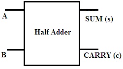
The digital electronic circuit that adds binary numbers is defined as half adder. The only difference in the process of addition is the digital system selected. Only 0 and 1 exist in the binary numbering system. The weight of the number depends entirely on the position of the binary number. Of these 1 and 0, 1 is regarded as the largest number and 0 as the smaller number. The block diagram of the adder is:
2、 Circuit diagram of half adder
The half adder consists of two inputs and produces two outputs. It is considered to be the simplest digital circuit. The input of the circuit is the bit on which addition is to be performed. The output obtained is sum and carry.
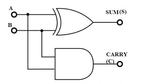
The circuit of the adder includes two gates. They are and and XOR gates. For both gates present in the circuit, the applied inputs are the same. But the output is taken from each door. The output of XOR gate is called sum, and the output of and is called carry.
3、 Semi additive truth table
In order to obtain the relationship between the obtained output and the applied input, a table called truth table can be used for analysis.
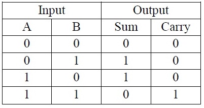
The following points can be clearly seen from the truth table above:
1. If a = 0, B = 0, that is, both inputs applied at the same time are 0. Then, the output sum and carry are both 0.
2. In the two inputs of the application, if someone inputs 1, sum is B E1, but carry is 0.
3. If both inputs are 1, sum equals 0 and carry equals 1.
4. Based on the applied input, the half adder continues the addition operation.
4、 Equation
The equation of such circuits can be realized by the concepts of product sum (SOP) and product sum (POS). The Boolean equation of such circuits determines the relationship between the applied input and the obtained output.
In order to determine the equation, the K diagram is drawn according to the truth table value. It consists of two equations because two logic gates are used. The K figure of carry is:
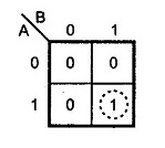
The output equation of carry is obtained from the and gate.
C = AB
The Boolean expression of sum is implemented in the form of SOP. Therefore, the K-map of sum is:
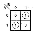
The determined equation is:
S =A⊕B
5、 Application field of adder
The application scenarios of this adder are as follows:
1. In order to perform addition on binary bits, arithmetic and logic units in computers prefer this adder circuit.
2. The combination of half adder circuits results in the formation of full adder circuits.
3. These logic circuits have advantages in the design of calculator.
4. If you want to calculate the address and table, you'd better use this circuit.
5. The circuit can not only add, but also deal with various applications in digital circuits.


