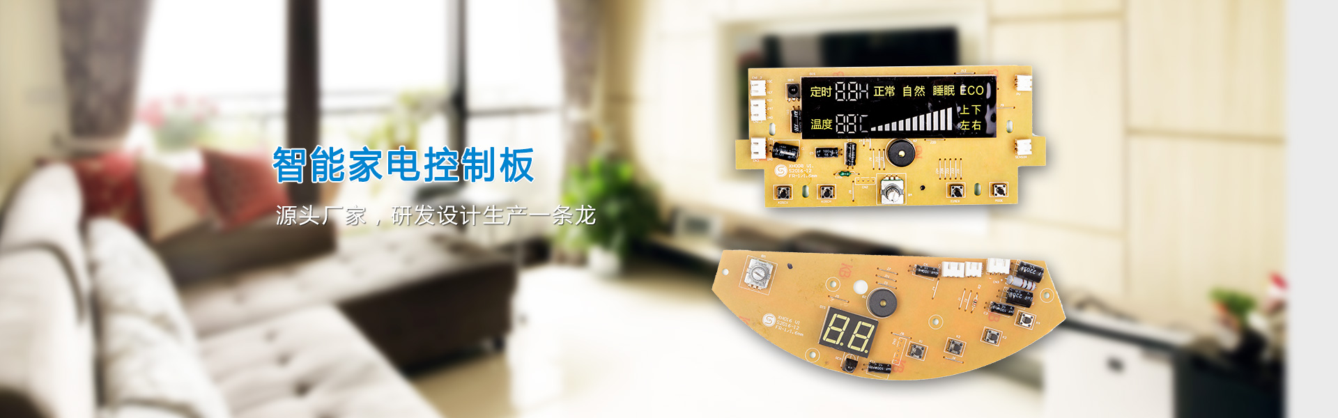
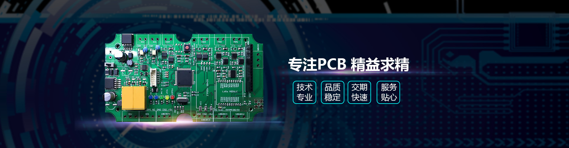
Industrial PCB Board multi layers vias with solder PCBA support Gerber BOM file

PCBA PROCESSING CAPABILITY
Turnkey PCBA | PCB+components sourcing+assembly+package+shipment |
Assembly details | SMT and Thru-hole, ISO SMT and DIP lines |
Lead Time | Prototype: 15 work days. Mass order: 20~25 work days |
Testing on products | Flying Probe Test, X-ray Inspection, AOI Test, Functional test |
Quantity | Min quantity: 1pcs. Prototype, small order, mass order, all OK |
Files needed | PCB: Gerber files(CAM, PCB, PCBDOC) |
Components: Bill of Materials(BOM list) |
Assembly: Pick-N-Place file |
PCB Panel Size | Min size: 0.25*0.25 inches(6*6mm) |
Max size: 20*20 inches(500*500mm) |
PCB Solder Type | Water Soluble Solder Paste, RoHS lead free |
| Passive Down to 0201 size |
BGA and VFBGA |
Leadless Chip Carriers/CSP |
Double-sided SMT Assembly |
Fine Pitch to 0.8mils |
BGA Repair and Reball |
Part Removal and Replacement |
Component package | Cut Tape,Tube,Reels,Loose Parts |